
OUR SERVICES
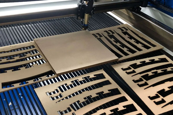
レーザーカッターで作れる部品は何ですか?
レーザー切断は、産業機器、コントロールパネル、ユーザーインターフェース、楽器、医療機器などで使用されるフェイスプレートの作成に最適です。 これは、ほぼすべての電子デバイスが何らかの筐体に収容されているエレクトロニクス業界に特に当てはまります。
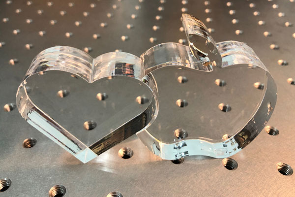
レーザー切断は、金属やプラスチックから小さな機械部品を作成するのにも最適です。 たとえば、複雑な機械装置で使用される小型歯車は、レーザー切断の低コストで高精度の機能を活用できます。
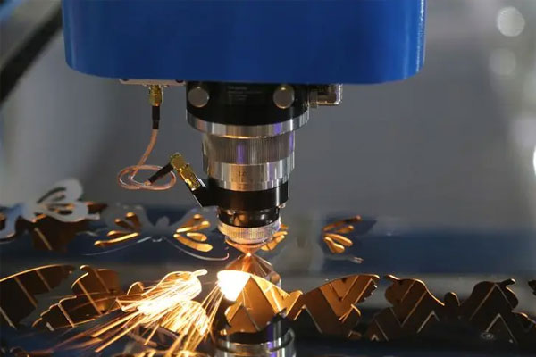
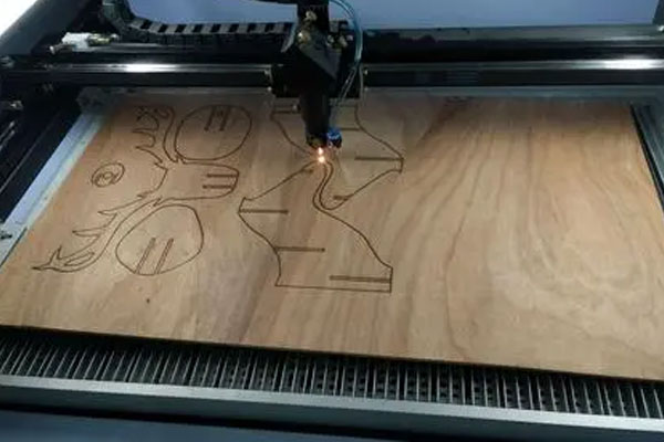
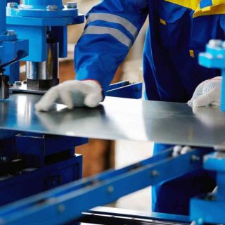
木材のレーザー切断は、美観が重要となる芸術的な用途での使用に最適です。 レーザー切断の高温により、切断端が焦げたような外観になり、木箱、デバイスの筐体、パターンの彫刻などで非常に人気のあるデザインに強いコントラストを生み出すことができます。 金属レーザー切断はブラケットやフィッティングの製造に使用でき、当社のレーザー切断サービスと金属曲げおよび仕上げサービスを組み合わせることで、市場で使用できる 3D 部品の作成が可能になります。
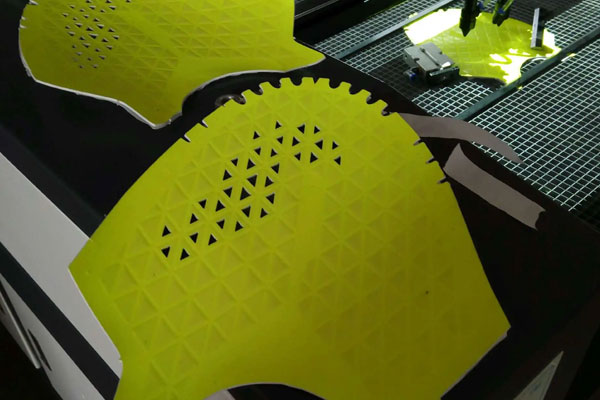
当社のレーザーカットカードストックとテキスタイルは、製品パッケージ、マテリアルインセット、カード、販促資料、デカールなどのファッションや工芸品に最適です。 フェルトなどの一部の繊維は、シールや O リングなどの工学用途にも使用できます。
レーザー切断は、金属やプラスチックから小さな機械部品を作成するのにも最適です。 たとえば、複雑な機械装置で使用される小型歯車は、レーザー切断の低コストで高精度の機能を活用できます。
木材のレーザー切断は、美観が重要となる芸術的な用途での使用に最適です。 レーザー切断の高温により、切断端が焦げたような外観になり、木箱、デバイスの筐体、パターンの彫刻などで非常に人気のあるデザインに強いコントラストを生み出すことができます。 金属レーザー切断はブラケットやフィッティングの製造に使用でき、当社のレーザー切断サービスと金属曲げおよび仕上げサービスを組み合わせることで、市場で使用できる 3D 部品の作成が可能になります。
当社のレーザーカットカードストックとテキスタイルは、製品パッケージ、マテリアルインセット、カード、販促資料、デカールなどのファッションや工芸品に最適です。 フェルトなどの一部の繊維は、シールや O リングなどの工学用途にも使用できます。


“当社は、全従業員の全面的なサポートを得てプロセスを継続的に改善し、品質を向上させ、それにより、いつでも時間通りに欠陥のない製品とサービスでお客様のニーズを満たすことに全力で取り組んでいます。”
– John Smith, BE-CU CTO
長持ち保証
ソリューション
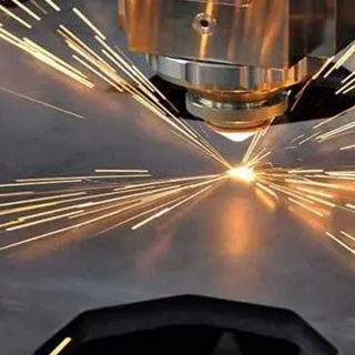
製造においては品質が不可欠です。 高い精度と精度で製造できない部品は信頼性が低くなります。 ただし、部品の経済性を確保するには、部品を迅速に製造することも不可欠です。 レーザー切断分野における当社の長年の経験により、当社は品質とスピードの完璧なバランスを見つけることができ、ソフトウェア主導のサービスによりお客様が必要とする部品を優れた価格で提供できるようになりました。
当社が製造する部品に対する自信を示すために、注文の規模、選択された材料、部品の複雑さに関係なく、すべての部品に 365 日の保証が付いています。 この保証により、エンジニアは、最初の注文からだけでなく、すべての注文のすべての部品について、部品の信頼性についてある程度の自信を得ることができます。


長年にわたる素晴らしいサービスとサポートにいつも感謝しています。 とても親切で、やり取りを楽しんでいるメーカーと仕事ができることに毎日感謝しています。
― Mariko Carandang
一流の製造パートナーをお探しですか?
さらに解決策を見つける
BE-CUのブログへようこそ
私たちは、ラピッドプロトタイピングおよび製造業界での長年の経験から学んだ情報、ヒント、物事を共有します。
答えを見つける / September 26-28
よくある質問
プロトタイプから完全な組み立てまで、あらゆる段階をサポートします。 15 を超える仕上げオプション、広範なハードウェア カタログなどをご用意しています。プロジェクトのすべてのニーズをカバーする幅広いサービスからお選びください。
6月 8, 2015業界
デジタル技術の統合により、板金業界は大きな変革を遂げ、プロセスを合理化し、精度を向上させ、金属部品の製造方法に革命をもたらしました。
12月 6, 2023製造技術
レーザー溶接は、高エネルギー密度のレーザー光線を熱源として使用する効率的で精密な溶接方法です。 高効率、正確さ、シンプルさ、使いやすさという利点があります。 現在、レーザー溶接は、電子部品、自動車製造、航空宇宙、その他の […]
12月 6, 2023製造技術
産業の発展に伴い炭素排出量は劇的に増加し、生活環境の質は低下しています。 炭素排出量を削減するために、世界中の国々が合意に達し、気候変動に関する国連枠組条約に署名しました。 中国は「2030年に炭素ピークに達し、2060 […]